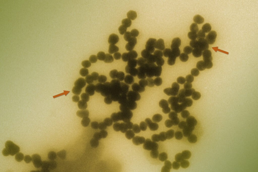
Nanotechnology is the understanding, manipulation and control of matter at the nanoscale, at sizes of about 1 to 100 nanometers, to produce new structures, materials and devices. A nanometer is one billionth of a meter, a scale at which a material can behave differently from the same material in bulk. The U.S. National Science Foundation (NSF) notes that nanotechnology appears in products as varied as carbon fiber tennis rackets, water purification systems, faster computer chips and solar panels.
History of nanotechnology
The idea is usually traced to the physicist Richard Feynman. In 1959 he gave a lecture at the California Institute of Technology titled “There’s Plenty of Room at the Bottom,” in which he imagined using machines to build smaller machines, down to the molecular level. The Japanese scientist Norio Taniguchi is credited with first using the word nanotechnology, in 1974, to describe processing materials one atom or one molecule at a time.
The field gained tools in the 1980s. In 1981 Gerd Binnig and Heinrich Rohrer invented the scanning tunneling microscope at the IBM Zurich Research Laboratory, which let researchers see and move individual atoms. In 1985 Robert Curl, Harold Kroto and Richard Smalley discovered fullerenes, or buckyballs, stable spheres made of carbon.
Quantum dots offer another milestone. According to the Royal Swedish Academy of Sciences, Aleksey Yekimov created size-dependent quantum effects in colored glass in the early 1980s, Louis Brus later proved such effects in particles floating in a liquid, and in 1993 Moungi Bawendi developed chemical production methods that gave nearly perfect particles. The three shared the 2023 Nobel Prize in Chemistry for the discovery and synthesis of quantum dots.
How nanotechnology works
Nanotechnology works because properties change at very small sizes. The Nobel committee explains that an element’s properties are normally governed by how many electrons it has, but when matter shrinks to nano dimensions, quantum phenomena arise that depend on the size of the particle. A quantum dot is a clear example: its color depends on its size.
Surface area also matters. A nanoparticle has a large fraction of its atoms on its surface compared with a larger piece of the same substance, so it can react faster or interact more strongly with its surroundings.
There are two broad ways to make nanoscale structures. Top-down methods start with a larger piece and carve or etch it down, as in the manufacture of computer chips. Bottom-up methods assemble structures from individual atoms or molecules, relying on chemistry and self-assembly. Instruments such as electron microscopes and scanning probe microscopes are needed to see and measure objects this small.
Types of nanomaterials
Researchers group nanomaterials by their shape and composition. Nanoparticles are small clusters of atoms, such as the quantum dots, metal particles and oxide particles used in coatings and sensors. Nanotubes and nanowires are long, thin structures; carbon nanotubes are rolled sheets of carbon atoms known for strength and electrical conductivity.
Thin films and layered materials are only a few atoms thick and are used in electronics and coatings. Nanoporous materials contain channels of nanometer width that can filter or trap substances. Fullerenes, discovered in 1985, are hollow carbon cages. Each of these is a type of nanomaterial, and many are built from carbon, though metals and semiconductors are also common.
Applications of nanotechnology
The Nobel committee reports that quantum dots now light computer monitors and television screens based on QLED technology, add nuance to the light of some LED lamps, and are used by biochemists and doctors to map biological tissue. It adds that researchers expect future uses in flexible electronics, tiny sensors, thinner solar cells and encrypted quantum communication.
Nanoscale features are central to modern electronics, since the transistors in a semiconductor chip are patterned at tiny dimensions. NSF also notes that nanotechnology advances are tied to new energy technologies, including solar panels, and to fields such as medicine, clean energy, manufacturing and agriculture. Nanoscale coatings, catalysts and filtration membranes are further examples already in use.
In medicine, the focus is on diagnostic tools and on carriers that deliver drugs to specific cells. Many of these uses are still being tested, and each product must pass the safety review that applies to its category.
The Nobel announcement adds that quantum dots can guide surgeons when they remove tumor tissue, a use that relies on their bright glow. Because a dot’s color depends on its size, makers can tune the color it emits by controlling how large the particles grow during synthesis, which is why the same material can produce red, green or blue light.
Advantages and disadvantages of nanotechnology
The main advantage is control. Designing a material at the nanoscale lets engineers tune its color, strength, conductivity or chemical activity in ways that bulk materials cannot offer. This can mean lighter materials, more efficient devices and more sensitive tests.
The disadvantages are mostly questions about safety and cost. Because nanomaterials can behave differently from larger forms of the same substance, their effects on human health and the environment cannot be assumed from older data, and researchers and regulators study them case by case. Manufacturing precise nanostructures at scale can also be expensive and difficult to reproduce consistently.
The word nanotechnology is sometimes applied loosely to marketing. Nanoscale size alone does not make a product safer or better, and claims should be judged by the evidence for the specific material.
Nanotechnology vs. nanoscience
Nanoscience is the study of phenomena and materials at the nanoscale, and nanotechnology is the use of that knowledge to build things. The two overlap heavily, and discoveries such as quantum dots moved from laboratory curiosity to everyday products within a few decades. The information here is general background and not advice about any product.
More in Materials Science
Key facts
- NSF defines nanotechnology as the understanding, manipulation and control of matter at sizes of about 1 to 100 nanometers to produce new structures, materials and devices.1
- Richard Feynman gave his "Plenty of Room at the Bottom" lecture in 1959, and Norio Taniguchi first used the term nanotechnology in 1974.3
- Binnig and Rohrer invented the scanning tunneling microscope in 1981, and fullerenes were discovered in 1985.3
- The 2023 Nobel Prize in Chemistry went to Bawendi, Brus and Yekimov for the discovery and synthesis of quantum dots.2
- Quantum dots now light QLED screens, add nuance to some LED lamps and are used to map biological tissue.2
Related concepts
Quick checkHow small is the nanoscale?Show answer
NSF describes the nanoscale as about 1 to 100 nanometers. A nanometer is one billionth of a meter, and at this size materials can show new properties that depend on particle size.
Sources
- 1. National Science Foundation, Nanotechnology (focus area), https://www.nsf.gov/focus-areas/nanotechnology
- 2. Royal Swedish Academy of Sciences, Press release: The Nobel Prize in Chemistry 2023, https://www.nobelprize.org/prizes/chemistry/2023/press-release/
- 3. Bayda et al., The History of Nanoscience and Nanotechnology: From Chemical-Physical Applications to Nanomedicine, Molecules (2020), PubMed Central, https://pmc.ncbi.nlm.nih.gov/articles/PMC6982820/
Editorially reviewed by Specialty Digest Editorial TeamLast reviewed November 4, 2026Researched and drafted with AI assistanceReport an issue